
A hands-on breakdown of the three most common bussing-related causes of center hole cell cracks during PV module lamination
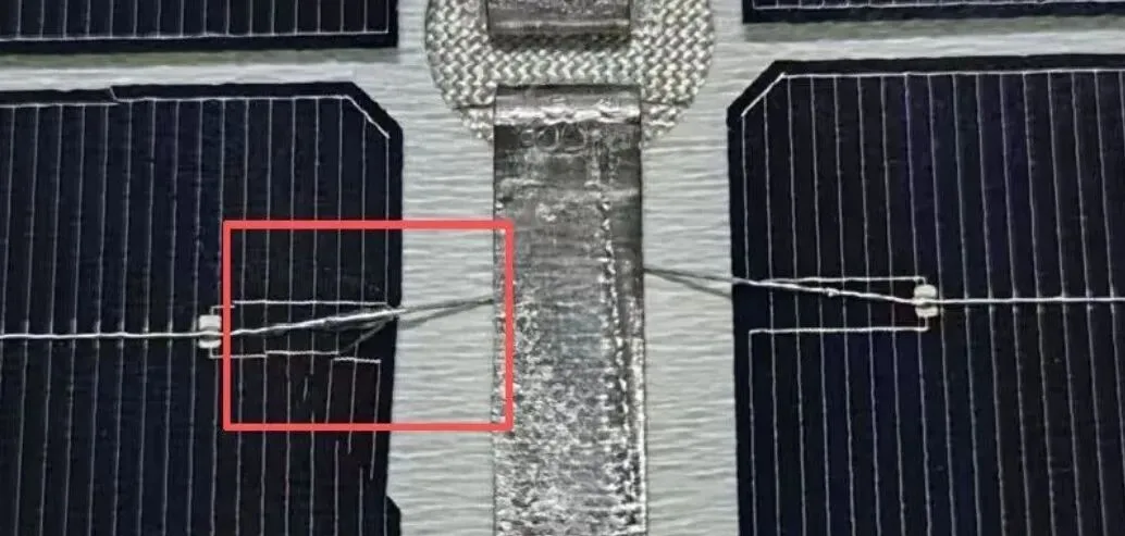
Quick answer: Centre-hole cracks are the most common cosmetic defect on a PV module line, and bussing — the overlap soldering that joins string ends — is the step that creates them. The failure path is mechanical rather than electrical: when ribbon is soldered across a cell edge, the joint shrinks as it cools and pulls on the silicon underneath, and a cell that is already thin or has a weak point at the centre hole cracks along that line. The geometry involved is small, with ribbon around 0.13 mm and module features near 35 mm, which is why the crack often starts invisibly and only shows up in electroluminescence. Reducing it is a matter of controlling the soldering thermal profile, the overlap length and the support under the cell during the joint, rather than of changing the ribbon.
PV Module Manufacturing · by Jerry, Ooitech
Product Introduction
Center hole cracks are the most frequent cosmetic defect you run into on a PV module line. The causes are messy and there are a lot of them. This post narrows things down and looks only at the center hole cracks that come from problems in the bussing (overlap soldering) step. Three typical root causes, walked through one at a time.
Technical Parameters
Reserved gap between ribbon and cell edge is too small
The cell edge sits too close to the bus bar.
TOPCon cell strings use a front-side ribbon positive structure, and the ribbon is soldered to the back of the bus bar. During bussing the machine does bring the cell and bus bar to the same plane, but the two materials differ a lot in thickness:
| Item | Thickness |
|---|---|
| Standard TOPCon wafer | 0.13mm |
| Middle bus bar | 0.35mm~0.4mm |
Once you get into lamination, the contact area where the ribbon meets the cell edge sees a two-way force.
When the gap between cell and bus bar is too small, the angle between the ribbon and the wafer edge shrinks. Pull force F1 drops, and vertical pressure F2 goes up at the same time.
Wafers are brittle. Under that higher pressure the edge cracks easily, and you end up with a center hole crack.
Technical Advantages
Ribbon bends and deforms after forming
If the plane difference between cell and bus bar is too large during bussing, the ribbon keeps a height difference after it's soldered.
Bussing has already fixed the total ribbon length. The extra length has nowhere to go, so the ribbon bends to absorb it. That bent ribbon then keeps pressing on the cell edge, and you get batch center hole cracks.
Solder ring defect during bussing (a rarer batch cause)
Here the cell and bus bar have a slight plane difference during bussing, and the harpoon area has no bus bar support, so the ribbon separates from the wafer. When the solder heat melts the ribbon coating, a raised ring of solder forms around it. During lamination pressure this hard solder ring pushes straight into the wafer and cracks it, giving another center hole crack.
Product Application
These three failure modes show up across most crystalline module lines, and they matter most on thin, high-efficiency cells where the mechanical margin is already tight. Watching ribbon-to-cell spacing, plane alignment during bussing, and solder profile control gives you the biggest lever on center hole crack yield.
Ooitech's View
Thin TOPCon wafers at 0.13mm leave almost no room for error, so the F1/F2 force balance we talk about here is really an alignment problem you solve upstream at the stringer and bussing stations, not something you can fix later in lamination. On the module lines we build, keeping the cell and bus bar coplanar and holding a steady solder profile is where most center-crack yield actually comes from. If you want to see how these steps run in a real factory, Ooitech's YouTube channel www.youtube.com/ooitech has plenty of line footage worth a look.