
How steel plate printing and local poly-silicon (poly finger) technology help TOPCon cut silver paste cost, boost efficiency to 26.09%
Quick answer: Steel plate printing combined with local poly-silicon fingers is one of the routes being explored to push TOPCon efficiency while reducing silver use. Steel plate printing replaces part of the screen-printed metallisation with a pattern that can be finer and more consistent than a mesh screen allows, and the local poly-silicon fingers define where the rear contact actually sits rather than covering the whole area. The reported results sit in the 26.09% to 25.8% efficiency band, with a 1.7% figure and a 90% yield class appearing in the data, and a 1% relative gain claimed over the comparison structure. The 58.9% figure relates to a process share in the analysis. The engineering attraction is that finer metallisation carries more current per unit of shading, which is exactly the trade every high-efficiency cell is fighting.
PV Module Manufacturing · by Jerry, Ooitech
Product Introduction
Last month I visited a TOPCon factory. Old Zhang, the process lead, was wiping his hands after swapping a fresh screen off the printer, doing the math out loud with me.
"One PI-film steel-wire screen runs 4,000 to 8,000 yuan, and across the industry the life is usually about 400,000 wafers. A good one hits 450,000, a bad one leaks paste at 300,000. Spread over each wafer that's a cent or two. You think I care about screen cost?"
He leaned against the tool cabinet by the printer and dropped his voice: "Silver paste is the real story."
Early 2023, silver ran around 6,000 yuan per kilogram, and silver paste was just 3.4% of module cost. By this January, paste had climbed to 29% of total module cost. Silver paste has formally overtaken polysilicon as the number-one cost driver in a PV module.
On June 23, spot silver was 15,233 yuan/kg, and front-side fine-grid silver paste quoted 15,779 yuan/kg.
"29 percent!" He slapped the cabinet door. "We break our backs on cost reduction and efficiency, and it's still less than a single day of silver price swing."
He pulled out his phone and showed me an internal chart: front-side silver paste unit price over the past three years, almost a straight 45-degree climb.
"Seen that steel-plate printing paper?" I asked.
"Read it. The Joule one from Ningbo Institute of Materials. The whole production line group chat passed it around. But management is still hesitating, because in the end, can this thing actually save money?"
As he said this, a screen printer nearby was pushing out the next batch, squeegee gliding silver paste across the screen at a steady pace, the vacuum hiss keeping rhythm.
It printed steady. Stable, reliable, high yield, workers who know it cold.
But everyone knows "stable" has never been a moat in this business.
This article answers one question: can steel plate printing plus local poly-silicon help TOPCon claw back some cost advantage in 2026, with silver prices this high?
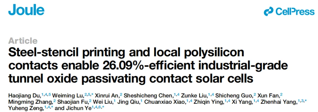
In January 2026, Joule published work from Ye Jichun's team at the Ningbo Institute of Materials, CAS. On industrial M10 wafers, they used steel plate printing to replace conventional screen printing for the front grid, and local poly-silicon to replace full-area poly for the rear contact. ISFH-certified efficiency: 26.09%.
That number isn't the industry record. JinkoSolar posted 26.4% in June 2026, and Trina had a 26.58% certification earlier. But the value here isn't the efficiency figure, it's that this paper tackles three TOPCon pain points at once: efficiency, silver reduction, and bifaciality. And both technologies are compatible with existing lines, not a tear-down-and-rebuild.
Let's open it up.
Technical Parameters
Grid Line Morphology: Screen vs Steel Plate Printing
| Metric | Screen Printing | Steel Plate Printing |
|---|---|---|
| Line width | 17.0-19.4 μm | 14.1-15.5 μm |
| Line height | 8.7 μm | 8.9 μm |
| Aspect ratio | 45.1% | 58.9% |
| Edge profile | Sloped | Near-vertical |
| Finger spacing | 1066 μm | 944 μm |
| Contact resistivity | higher | 2.4 mΩ·cm² (~15% lower) |
Local Poly-Silicon vs Full-Area Poly (30% coverage)
| Metric | Full-Area Poly | Local Poly-Silicon |
|---|---|---|
| Jsc | 41.90 mA/cm² | 42.09 mA/cm² |
| J0 (saturation current density) | 8.76 fA/cm² | 6.40 fA/cm² (-27%) |
| Bifaciality | 84.26% | ~90% |
| Voc | 724.9 mV | 729.9 mV |
| Efficiency | ~25.8% | 26.09% |
| LCOE reduction | baseline | -1.7% |
Technical Advantages
One: Steel Plate Printing Is More Than Swapping a Screen
Conventional TOPCon front grids use screen printing, where a woven mesh scrapes silver paste onto the wafer. That woven mesh has knots where warp and weft cross, and paste transfers through the gaps between them. Those knots dictate the grid shape: wide, short, sloped edges.
Steel plate printing uses a full-open metal stencil, the same class of tech Tongwei calls "full-open steel plate printing." No weave. Paste extrudes straight through slots opened by laser or electroforming. The grid shape changes instantly:
- Screen printing: 17.0-19.4 μm wide, 8.7 μm tall, aspect ratio 45.1%, sloped edges.
- Steel plate printing: 14.1-15.5 μm wide, 8.9 μm tall, aspect ratio 58.9%, near-vertical edges.
3-4 μm narrower, 0.2 μm taller, aspect ratio from 45% up to 59%.
Three changes, three accounts to settle:
First, less shading. Narrower fingers, more open area for light. That 0.1% absolute efficiency gain comes from these 3-4 microns.
Second, less silver. Take a 210R cell. June 2026 field data shows mainstream TOPCon makers already at 78.5-85.5 mg/wafer, industry average around 83 mg/wafer. With steel plate screens, the main use right now is on the rear busbar/finger, cutting 3-5 mg per wafer.
3-5 mg sounds small, but multiply by line volume and it adds up. At the current paste price of about 15,779 yuan/kg, saving 3-5 mg per wafer is about 0.047-0.079 yuan/wafer. A line running 500,000 wafers a day saves 23,500-39,500 yuan a day, or 7 to 12 million yuan a year (over 300 days).
And that's just the rear finger drop. As the process matures, steel plate printing is moving toward the front busbar and fine grid too, with more silver savings ahead.
Third, it makes the high-sheet-resistance emitter route work. Steel plate fingers can pack tighter. In the paper, spacing shrank from 1066 μm to 944 μm. Denser fingers mean shorter lateral carrier travel, so tolerance for emitter sheet resistance rises. The paper's simulation shows that as emitter sheet resistance climbs from 300 to 600 Ω/sq, the steel plate advantage widens from 0.09% to 0.12%.
This is a textbook case of structure changing the process window: steel plate printing isn't just a printer swap, it unlocks new emitter design space.
On the cost and life of the steel plate stencil itself, here's the account the line cares about most:
- Conventional PI-film steel-wire screen: 4,000-8,000 yuan each, life around 400,000 wafers.
- Steel plate stencil (current rollout stage): unit price more than 50% cheaper than PI-film (2,000-4,000 yuan range), but life is only about 200,000 wafers right now. A good one hits 200,000, a bad one gets replaced at 150,000.
Screen amortization: PI-film about 0.01-0.02 yuan/wafer, steel plate about 0.01-0.02 yuan/wafer. They break even. The steel plate advantage isn't in the screen, it's in silver savings: 3-5 mg per wafer on the rear finger, about 0.047-0.079 yuan/wafer, far bigger than the amortization gap.
But steel plate life is only half of PI-film, meaning double the change frequency, double the downtime, double the labor. Whether the silver savings cover the hidden cost of more frequent changes depends on how full your line runs. For fully loaded top players, the math works. For under-utilized lines, steel plate may not pay off. That's exactly why Tongwei and Jietai, with strong in-house cell absorption, dared to move first. Scale dilutes the short-life weakness.
Two: Silver-Silicon Contact, the Extra 0.4% Fill Factor Steel Plate Printing Throws In
Narrower fingers explain less shading and less silver. But steel plate printing hands over one more gain: contact resistivity drops about 15%. Measured in the paper: 2.4 mΩ·cm², well below screen printing, directly worth a 0.4% fill factor (FF) gain.
Why does swapping a screen make contact better?
The paper ran a full morphology analysis. After etching away the silver grid with nitric and hydrofluoric acid, they looked at the silver particles left on the silicon surface. Steel plate samples had noticeably higher particle density, sized 20-40 nm, more evenly spread. TEM further showed the steel plate samples formed a denser, continuous silver nanoparticle network in the glass layer at the silver-silicon interface.
Those silver nanoparticles are the conduction path. Electrons don't have to cross high-resistance glass; they hop straight between the silver particles.
The clearest evidence comes from scanning spreading resistance microscopy (SSRM). This technique literally "sees" the resistance distribution: a cross-section scan from silicon to silver grid, high-resistance zones bright, low-resistance zones dark. The steel plate sample's interface transition zone is narrower and darker, so interface resistance really is lower.
Print method → silver particle distribution → interface resistance → fill factor. Every step of that causal chain is backed by data.
LECO (Laser Enhanced Contact Optimization) is already an industry standard, expected to cover about 600 GW of TOPCon capacity. But even with the same LECO treatment, steel plate printing still cut contact resistance by another 15% over screen printing. That says steel plate printing has a native interface-quality edge that LECO can't level out.
Three: Local Poly-Silicon, Removing What Shouldn't Be There (the Rear Poly-Finger Technology)
Full-area poly-silicon on the TOPCon rear is a double-edged sword.
The good edge: extremely high passivation quality, one of the most mature passivated-contact schemes around.
The bad edge: poly absorbs light. Its parasitic absorption in the near-infrared eats light that should have become current. The direct result: short-circuit current (Jsc) can't rise, bifaciality can't climb. TOPCon bifaciality usually sits at 80%-85%, while heterojunction reaches 90%-95%.
The paper's idea is blunt: keep poly only where the electrode needs contact, replace the rest with AlOx/SiNx.
The path is laser plus wet etching:
- Deposit full-area poly-silicon (150 nm)
- 532 nm picosecond laser patterns the areas to remove
- The laser modifies the local phosphosilicate glass (PSG)
- KOH alkaline solution selectively etches away the poly in the irradiated zones
- About 30% of the area keeps poly as contact points
The cross-section SEM in the paper is clean: the poly edge shows a 2.7 μm step, a vertical face left after the poly is fully removed, with no visible laser damage residue. That means the selective-etch precision is good enough.
So what happens when coverage drops from 100% to 30%?
Stacked together, the paper puts the LCOE reduction at 1.7%. In PV, a 1.7% LCOE gap is the line between order wins, capacity utilization, and profit level.
Four: The Core Tradeoff, Contact Area vs Passivation Area on a Seesaw
Local poly design is essentially a seesaw problem:
- More poly coverage → better contact, smoother carrier transport → but more parasitic absorption, lower bifaciality.
- Less poly coverage → less parasitic absorption, higher bifaciality → but higher contact resistance, hindered carrier transport.
The paper found the balance with a systematic sweep: coverage from 20% to 100%, measuring passivation (J0) and contact resistivity (ρc), then Quokka 3 simulating efficiency at each coverage.
Efficiency peaks near 30% coverage. Below 30%, the contact-resistance penalty outweighs the parasitic-absorption gain; above 30%, the parasitic-absorption penalty outweighs the contact-resistance gain.
The simulation curve has a stable, wide plateau around 30%. Coverage drifting between 25% and 35% won't swing efficiency wildly. That wide process window is good news for mass production.
Product Application
Line Translation: Two Tables You Can Walk Away With
Process Knob One: Steel Plate Printing
| Dimension | Data | Line Meaning |
|---|---|---|
| Efficiency gain | +0.1% abs (paper) | A gain you get just from swapping the screen |
| PI-screen silver use (210R) | 78.5-85.5 mg, avg 83 mg | June 2026 field data |
| Steel-plate silver saving (rear finger) | 3-5 mg/wafer | ~0.047-0.079 yuan/wafer |
| Annual silver saving (500k/day line) | ~7-12 million yuan/year | Over 300 days, paste at 15,779 yuan/kg |
| PI-film screen | 4,000-8,000 yuan, 400k life | Current baseline |
| Steel-plate stencil | 2,000-4,000 yuan, ~200k life | Change frequency doubles, downtime must be counted |
| Overall economics | Silver saving vs screen amortization | Break-even; fully loaded lines pay off, under-loaded be careful |
| High-sheet-R emitter fit | Bigger gain at 600 Ω/sq | Evaluate emitter optimization in parallel |
Process Knob Two: Local Poly-Silicon
| Dimension | Data | Line Meaning |
|---|---|---|
| Efficiency gain | ~+0.3% abs | Larger than steel plate printing |
| Bifaciality gain | 84% → 90% | 5%+ rear generation gain |
| LCOE reduction | 1.7% | Overall economic account |
| New equipment | Picosecond laser + KOH wet etch | New process steps |
| Per-GW new capex | ~15-20 million yuan (industry estimate, not disclosed in paper) | Investment planning |
| Yield | Lab conditions >96% | Needs verification after transfer to production |
| Line compatibility | Medium (adds laser + wet etch) | Higher threshold than steel plate printing |
Contact and Notes
A Few Pits to Watch
First, run the steel-plate life math carefully. Half the price, but half the life. The rear finger saves 3-5 mg per wafer, about 0.047-0.079 yuan, enough to cover the amortization gap. But double the change frequency brings downtime, labor, and re-tuning cost that can swallow the silver savings on an under-utilized line. Fully loaded plants go first; under-loaded plants do the math before moving.
Second, laser damage control on local poly is the core difficulty. The paper uses a 532 nm picosecond laser. Energy density, scan speed, spot overlap, all need tuning for different wafer quality. The paper says laser damage is "completely eliminated" by wet etching, but in a production floor, equipment stability, incoming-material consistency, and ambient temperature and humidity swings can all discount that "complete elimination."
Third, no one has verified yield after stacking both technologies. Steel plate printing plus local poly plus high-sheet-resistance emitter, three variables tuned at once, and the process window narrows. The 26.09% was reached under controlled lab conditions, and yield may drop again when moved to production. This is the shared problem of every new tech introduction.
Tongwei is already in mass production, and Jietai is following in step. But between "mass-producible" and "you'll make money running it" lies a whole line's worth of conversion capability.
The biggest value of this paper isn't the 26.09%, which Jinko and Trina will soon overwrite with new records.
Its value is this: TOPCon's next upgrade direction now has two data-verified paths. One is low difficulty with steady returns (steel plate printing), one is higher threshold with bigger payoff (local poly-silicon). Which you pick depends on which path matters more to you right now.
Ooitech's View
What strikes me most is that both of these paths land back on the cell side, yet the pressure lands squarely on the module line downstream. Narrower fingers and higher bifaciality change how strings behave during tabbing, layup, and lamination, so if you're building or upgrading a TOPCon module line, your stringer tension, bifacial IV testing, and sun simulator setup need to keep pace, not lag. We've seen plenty of factories chase cell efficiency records while their module line quietly bleeds yield on the new geometry. If you want to see how a real production line handles these changes, the Ooitech YouTube channel at www.youtube.com/ooitech is worth a subscribe.